Why a LUT Is Programmable: Twenty Transistors, Sixteen Functions
Stephan Bökelmann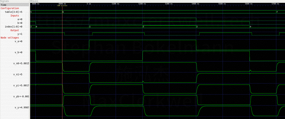
In the heart of almost every mainstream FPGA sits a wonderful piece of technology. Built from a handful of transistors, it holds the representation of every Boolean combination its inputs can produce, and it hands you the right one through a multiplexer. Xilinx shipped it in 1985, in the XC2064, the first commercial FPGA, and it is called a look-up table, a LUT.
In WTF are FPGAs I described it as “a small block of SRAM that implements any boolean function of N inputs by storing the truth table directly” and then moved on, because that article was about the chip, not the cell. The sentence has been bothering me ever since, especially after a few people on Instagram pointed out that the explanation was incomplete. Of course it was. It was an educational reduction, and I would write it that way again in an overview of a whole chip. But it did not let me sleep well, because the reduction hides exactly the part that makes a LUT interesting. It is correct, and it explains nothing. Why does storing a truth table make a circuit programmable, when wiring up gates does not? What does the storing actually look like in silicon? I wanted that in terms anyone can follow, and I did not have them yet.
So I built one. A look-up table with two inputs, from 20 MOS transistors, described in Python with SKiDL, drawn as a hierarchical KiCad schematic, simulated with ngspice, and dumped to a VCD file that opens in GTKWave. Everything is in lut-from-transistors, along with a paper that does the arithmetic in full.
This article is the short version of the argument: why the LUT is the structure it is, and why that structure is the thing that can be reprogrammed.
A Function Is Its Truth Table, and Nothing Else
Start with the part that feels too obvious to state. A Boolean function of two inputs is completely described by four output bits. Not mostly described: completely. Whether I write f = A AND B or f = NOT(NOT A OR NOT B) makes no difference to the table, and two expressions with the same table are the same function. There is nothing else about f to know.
Formally, a Boolean function of two inputs is a mapping f: {0,1}² → {0,1}. The domain is the four possible combinations of the inputs, the codomain is the two values an output bit can take. Because the domain is finite, the whole mapping can be written out, and what you write out is the truth table. “A function is its truth table” is therefore not a simplification, it is the definition. It also makes the counting below trivial: the number of mappings is |codomain|^|domain|.
Boole gave us the algebra in 1854; Shannon showed in 1938 that it describes switching circuits exactly. From that point on, a Boolean function and a circuit of switches are two views of one object. I traced that chain, from Aristotle through Llull, Leibniz and Boole to Shannon, in From Aristotle to the Bit; this article picks it up at the point where the algebra becomes transistors.
Now count. A function of k inputs has a truth table of 2^k rows, each row holding one bit that can be chosen independently of every other. So the number of distinct functions is 2^(2^k). For two inputs that is 16. Sixteen functions, and you know most of them by name:
| Table (T3 T2 T1 T0) | Function |
|---|---|
| 0001 | NOR |
| 0110 | XOR |
| 0111 | NAND |
| 1000 | AND |
| 1001 | XNOR |
| 1110 | OR |
The usual engineering approach is to pick one of those functions and build a circuit for it. A NAND gate is four transistors arranged so that the output is low exactly when both inputs are high. It is small, it is fast, and it is a NAND gate forever. Changing it into an XOR gate means a different arrangement of transistors, which means a trip back to the foundry.
The LUT takes the other road. Do not compute the function. Store it, and look it up.
That inversion is the whole idea, and it has an immediate consequence: if the function lives in four bits of storage rather than in the topology of the wiring, then changing the function means changing four bits. The hardware does not move.
Shannon’s Expansion Makes the Structure Inevitable
“Look it up” is still a slogan. What circuit looks something up?
Take any function f(A, B) and split it on one variable:
f(A, B) = (NOT A) · f(0, B) + A · f(1, B)
This is Shannon’s expansion. Check it by cases: if A = 0 the first term survives and gives f(0, B); if A = 1 the second gives f(1, B). It holds for every Boolean function, no exceptions, and it is not a simplification; the two halves f(0, B) and f(1, B) are themselves functions of one variable, and you can expand each of them on B until you are left with constants. Those constants are the four table bits.
Read the identity as hardware and it says: select between two sub-results according to A. A circuit that selects one of two inputs according to a control signal is a 2:1 multiplexer. So the expansion does not merely permit a multiplexer tree, it forces one, with one level per input variable:
T0 --[A=0]--+
            +-- N0 --[B=0]--+
T1 --[A=1]--+               +-- YI --|>o--|>o-- Y
T2 --[A=0]--+               |
            +-- N1 --[B=1]--+
T3 --[A=1]--+
Four stored bits enter on the left. The first level, selected by A, picks one bit out of each pair. The second level, selected by B, picks one of those two. The table index is 2·B + A, which is exactly the binary number formed by the inputs. The two inverters at the end are the output buffer; more on them shortly.
This is the entire logical content of a 2-input LUT: a binary tree of multiplexers, with the truth table at the leaves and the inputs as the steering signals. A 4-input LUT in a real FPGA is the same drawing with four levels and 16 leaves. Scaling is depth, not cleverness.
And now the programmability is no longer a slogan. The four leaves are data. Feed in 0110 and the circuit is an XOR gate. Feed in 1000 and the same transistors are an AND gate. In my simulation the four bits are literally voltage sources, 0 V or 5 V, which has the nice property that the function of the LUT can be read off the schematic.
In an FPGA they are SRAM cells, and the pattern written into them comes from the bitstream. That is the concrete meaning of configuring an FPGA: the bitstream is, among other things, the concatenated truth tables of every LUT on the die, and loading it is writing those bits into the configuration memory. Nothing in the silicon decides what function a LUT performs. The bitstream does.
Which puts the responsibility somewhere specific. When you write y <= a xor b; in VHDL, nothing in the chip knows about XOR. A synthesiser decides that this expression fits into one LUT, a technology mapper decides which LUT, and the bitstream generator decides which four bits to emit for it. Getting 0110 rather than 0111 into the right cell of the right logic element is the job of the toolchain, and it is a job you cannot inspect by looking at the hardware, because the hardware is identical either way. The transistors cannot be wrong. The bits can, and the only thing standing between your source and the correct bits is the tool. That is also why bitstream-level verification and reproducible toolchains matter at all, a thread I pulled on from the other end in From Bitstream to Idea.
Down to the Transistor: Why One Switch Is Not Enough
A multiplexer is two switches. A switch is a MOS transistor. That is where the interesting failure lives.
Use a single NMOS as the switch. Hold its gate at the supply, 5 V, and pass a 0 through it: the source sits at 0 V, gate-to-source is the full 5 V, the channel is wide open, the 0 arrives intact. Now pass a 1. As the output node rises, the gate-to-source voltage shrinks. The moment it reaches the threshold voltage the channel closes. The transistor stops conducting at
V_out = V_gate - V_threshold = 5 V - 1 V ≈ 3.5 V
(the 3.5 V rather than 4 V because the body effect raises the threshold as the source rises above bulk). So an NMOS pass gate delivers a weak, degraded 1. A PMOS has the mirror-image problem: clean 1s, degraded 0s.
Put the two in parallel, driven by complementary select signals, and each covers the other’s weakness. That is a transmission gate, and it is why the switch count doubles:
| Part | Transistors |
|---|---|
| 6 switches, 2 transistors each | 12 |
| 2 inverters for the input complements AN, BN | 4 |
| output buffer, 2 inverters | 4 |
| total | 20 |
Twenty transistors, and only 12 of them are the mux tree. Four exist purely to produce the complements the transmission gates need, and four more to fix a problem the tree creates.
That problem: a chain of pass transistors is not a gate. It does not drive, it merely connects. The internal node YI is at the end of up to two switches in series, it has no path to the supply of its own, and its drive strength depends on how many switches are in the path. A CMOS inverter restores it, with its output hard-connected to supply or ground, and a second inverter restores the polarity. Hence two, not one. The buffer is not a decoration; without it the LUT could not drive another LUT.
The voltage at which the first inverter stops calling its input a 1 and starts calling it a 0 is its switching threshold V_M, and it is worth computing, because it is the number that decides the glitch behaviour later. Set the two drain currents equal at the point where output equals input, and with r = sqrt(k_p/k_n) you get
V_M = (V_Tn + r·(V_DD - |V_Tp|)) / (1 + r)
My PMOS is half as strong as my NMOS, so r = sqrt(0.5) = 0.707 and V_M = 2.24 V. That is noticeably below the 2.5 V midpoint, because the weaker PMOS needs a lower input, and so a stronger PMOS drive, to balance the NMOS. A symmetric inverter would have the PMOS twice as wide. I did not do that, and 2.24 V is the consequence. Remember the number.
What the Simulation Says
One transient run of 12.8 µs steps the inputs through all four combinations in Gray code (index 0, 1, 3, 2, so only one input changes at a time) and rewrites the table bits every 800 ns, which is this circuit’s version of loading a new bitstream. All 16 functions, 64 of 64 truth table entries, in a single run. All correct.
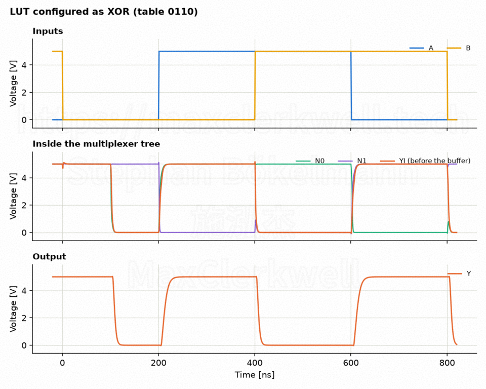
The plot shows one function window out of the sixteen. During the first 100 ns the table still holds the previous function; it is rewritten at 100 ns.
| Quantity | Value |
|---|---|
| Level of internal node YI for a 1 | 5.00 V |
| Level of output Y for a 1 | 5.00 V |
| Supply current at rest, largest | 0.015 µA |
| Delay A to Y, rising / falling | 12.2 ns / 9.1 ns |
| Delay B to Y, rising / falling | 10.8 ns / 7.8 ns |
| Delay table bit to Y, rising / falling | 11.1 ns / 8.2 ns |
Three things in that table are worth more than their row height.
The transmission gates earn their transistors. YI reaches a full 5.00 V, not 3.5 V. The first inverter of the buffer is therefore fully switched, neither of its transistors is left half-on, and the circuit draws 15 nanoamps at rest instead of the milliamps a half-open inverter would burn. The doubled switch count buys static power.
LUT inputs are not equal. B steers the last mux level and passes through one switch; A steers the first and passes through two. B is about 1.4 ns faster. This is not an artifact of my generic models; it is a structural property of a mux tree, and it is why real synthesis and place-and-route tools track per-input delay and route timing-critical signals to the fast pins of a LUT. A fact I had read as a tool heuristic turns out to fall straight out of Shannon’s expansion.
Reconfiguration is not special. A table bit reaches Y in 11.1 ns, essentially the same as A. From the circuit’s point of view a configuration bit and an input are both just signals entering the tree at different depths; “programming” is electrically unremarkable. The distinction between data and configuration is one we impose, not one the hardware observes.
A Glitch That Does Not Make It Out
One more experiment, because the mux tree has an honest hazard. If both inputs change at the same instant, the tree passes through an intermediate state, even when the old and the new table entry are identical and the output should not move at all.
| Change | Lowest YI | Lowest Y |
|---|---|---|
| XOR, index 1 to 2 | 3.37 V | 5.00 V |
| XOR, index 2 to 1 | 3.58 V | 5.00 V |
| XNOR, index 0 to 3 | 3.14 V | 5.00 V |
| XNOR, index 3 to 0 | 3.74 V | 5.00 V |
The internal node dips by up to 1.9 V, and the output does not move at all. Now use the number from the buffer section. The first inverter switches at V_M = 2.24 V. The deepest dip at YI, in the XNOR case, reaches 3.14 V. The dip therefore stays 0.90 V above the switching threshold, the inverter never leaves its logic-high region, and there is nothing at its output to filter in the first place.
That is worth being precise about, because the obvious explanation is the wrong one. It is tempting to say the 10 pF at the output smooths the glitch away. It does not. The 10 pF is there to represent what the LUT drives, not to suppress anything, and in these four cases the buffer never begins to respond, so the load is irrelevant to the outcome. The hazard is defeated by threshold margin at the buffer’s input, not by capacitance at its output. The glitch is entirely real inside the multiplexer tree and entirely invisible after one restoring stage.
Which also tells you how the margin could be lost. Make the PMOS of that first inverter wider and V_M moves up toward 2.5 V, eating 0.26 V of the 0.90 V margin. Add series resistance in the tree, or more levels for a wider LUT, and the dip goes deeper. Somewhere those two curves cross, and then the glitch does propagate, and the 10 pF starts to matter after all because it sets how wide the surviving pulse is. None of that is a theorem about LUTs, it is a sizing exercise about this one. Which is a decent illustration of why “it simulated fine” is a statement about a model, not about silicon.
The Schematic Is Generated, and Checked
A note on method, because it changed how I work.
The circuit is written once, in Python. hier.py walks the hierarchy and emits both a flat SKiDL circuit and five KiCad sheet files (lut2, inverter, mux2, switch, buffer) which instantiate into 15 sheets, three levels deep, so the transistors of a switch live at lut2 / mux_n0 / sw0. Then kicad-cli exports a flat SPICE netlist from the schematic, and that netlist is what ngspice simulates.
The pipeline is:
SKiDL (lut.py) -> KiCad schematic -> ngspice -> VCD -> GTKWave
The step I care about is the comparison in the middle. generate.py ends by printing
schematic <-> SKiDL netlist: IDENTICAL
which asserts that the drawing a human reads and the code that generated it describe the same circuit, and CI fails if they ever diverge.
The schematic is not documentation drifting alongside the design; it is a build artifact of it. Having worked on enough projects where the schematic PDF and the shipped board are two different opinions, I find this worth the plumbing.
The repository is archived on Zenodo and citable: the concept DOI 10.5281/zenodo.23089021 always resolves to the latest release.
The VCD output is the other small pleasure. VCD is a digital format, but it also carries real numbers, and GTKWave will draw those as analog traces. So one waveform window holds the table as a hex vector, the inputs and output as logic signals, and the node voltages v_n0, v_n1, v_yi, v_y as curves underneath: the digital abstraction and the analog reality it rests on, stacked on the same time axis. The writer is about 100 lines with no dependencies. That is the view at the top of this article: the window from 4.8 µs to 5.6 µs, where the table changes from 5, NOT A, to 6, XOR, at the marker, and y then follows the table entry as the index steps through 0, 1, 3, 2.
What This Does Not Show
Honesty about the model, since the numbers above look more authoritative than they are:
- The transistor models are generic. Level-1 MOS, threshold 1 V, 10 µm × 10 µm channel, 0.5 pF junction capacitance. They describe no real part and no real process. A LUT in a modern FPGA switches in tens of picoseconds, not tens of nanoseconds; the ratios here are meaningful, the absolute numbers are not.
- The configuration is ideal. Voltage sources have no output resistance and cannot be disturbed by what they drive. SRAM cells can be, and must be sized for it.
- No layout. No wiring resistance or capacitance, one lumped 10 pF load.
- Four-terminal transistors. Every bulk is tied to its rail, as on a chip. Discrete three-terminal MOSFETs tie bulk to source inside the package, and their body diode will conduct in a transmission gate. If you want to build this on a breadboard, use a CD4007 or similar array with a separate bulk pin.
The Point
A gate computes one function because its wiring is that function. A LUT computes any function of its inputs because its wiring is a selector, and the function lives in storage the selector reads.
I have to stop at that word. At this point in my career I have an honest problem with “to compute”, and it has been getting worse rather than better: the deeper I get into computing, the more it all just looks mechanical to me. Every layer I open turns out to be charge moving and thresholds being crossed, and “computation” names no extra ingredient I can point at. Nothing in this circuit is doing anything beyond obeying its own physics. The computing seems to appear only when I show up and decide to read 5 V as a 1, call the pattern 0110 a function, and name that function XOR. Take me away and there is a 10 pF capacitor being charged and discharged. The word also quietly imports intention, which is how we end up saying a circuit “decides” or “figures out” something, and I think that habit is responsible for a large share of the confusion people have about what AI is. And it is suspiciously universal: if everything sufficiently intricate can be said to compute, then a river and a LUT and a brain all compute, and the term has stopped distinguishing anything at all.
This is not a problem the LUT created. It is just where the thought surfaced, because I had spent a week with twenty transistors that very clearly only move charge. But I do not have an answer, and I have started to think I need to go after the actual meaning of that word properly rather than keep using it as a placeholder. If you want to start where I am going to start: John Searle argued that computation is observer-relative, something we ascribe to a physical system rather than discover in it, and Hilary Putnam’s triviality argument claims that under a sufficiently permissive mapping almost any open physical system can be said to implement almost any computation. If either of those holds up, then “this circuit computes XOR” is a statement about me, not about the circuit. That is a different article, and probably a longer one. It would be the same complaint I made about physics in Physics Doesn’t Explain Anything, moved one floor down: we have an exact description of what the circuit does, and I keep mistaking the description for an explanation of what it is.
Reprogramming an FPGA is not, at this level, a mysterious act. It is writing new leaf values into a few hundred thousand multiplexer trees. The transistors never move. Everything else about an FPGA, the routing fabric, the bitstream format, the place-and-route tooling, is scaffolding around that one substitution of storage for topology.
Twenty transistors, four bits, sixteen functions. The full derivation, with every number computed from the transistor model and every figure regenerated from the simulation results, is in the paper in the repository. Clone it, run uv run generate.py and uv run simulate.py, and open the result in GTKWave. Watching the same transistors turn into sixteen different gates, one every 800 nanoseconds, makes the argument better than this article does.