Why Does Copper Conduct? A Tour for Non-Physicists
Stephan BökelmannI recently finished a small paper that derives the electronic structure of solids step by step, aimed at first-year physics students. This post is the version without the mathematics: the story you can follow on a train ride. If you want the full derivations, the paper is linked at the end.
A Question That Sounds Trivial
Why does copper conduct electricity and diamond doesn’t?
The answer you probably learned in school, “metals have free electrons”, is not wrong, but it quietly dodges the real question. A gram of diamond contains roughly as many electrons as a gram of copper. Nobody nailed them down. So why are the electrons in copper “free” and the ones in diamond not? What, physically, is the difference?
It turns out the answer has nothing to do with electrons being loose or stuck. It has to do with seating.
One Atom: a Staircase, Not a Ramp
Quantum mechanics makes one claim from which everything else follows: an electron bound to an atom cannot have just any energy. It can sit on step one, step two, step three, but never in between. The energy landscape of an atom is a staircase, not a ramp.
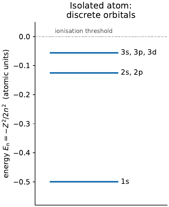
On top of that comes a rule with enormous consequences, the Pauli principle: each step seats at most two electrons. Electrons fill the staircase from the bottom, two per step, and then the box office closes.
Two Atoms: Every Step Splits in Two
Bring two atoms close together and something curious happens. An electron that belonged to one atom starts to notice the neighbor. Quantum mechanics allows it to tunnel across, and once the two atoms are close enough, the honest description is no longer “an electron at atom A” or “an electron at atom B” but a wave spread out over both. There are two ways to build such a shared wave: a smooth way, and a way with a kink in the middle. Kinks cost energy. So every single step of the staircase splits into a pair of steps, one slightly lower (the smooth, “bonding” arrangement) and one slightly higher (the kinked, “antibonding” one).
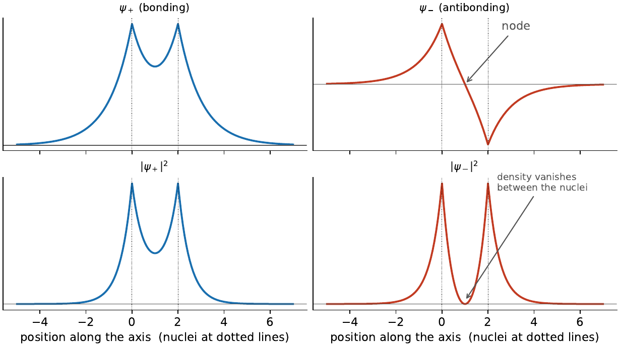
That’s it. That is the entire mechanism. The rest is repetition.
A Crystal: Steps Blur into Bands
A crystal is not two atoms but something like $10^{23}$ of them. Each original step now splits $10^{23}$ ways. The resulting levels are spaced so absurdly finely, roughly $10^{-23}$ electron volts apart, that they stop being steps at all. They blur into a continuous band of allowed energies. Between the bands there may remain forbidden zones, so-called band gaps, where no electron can sit, period.
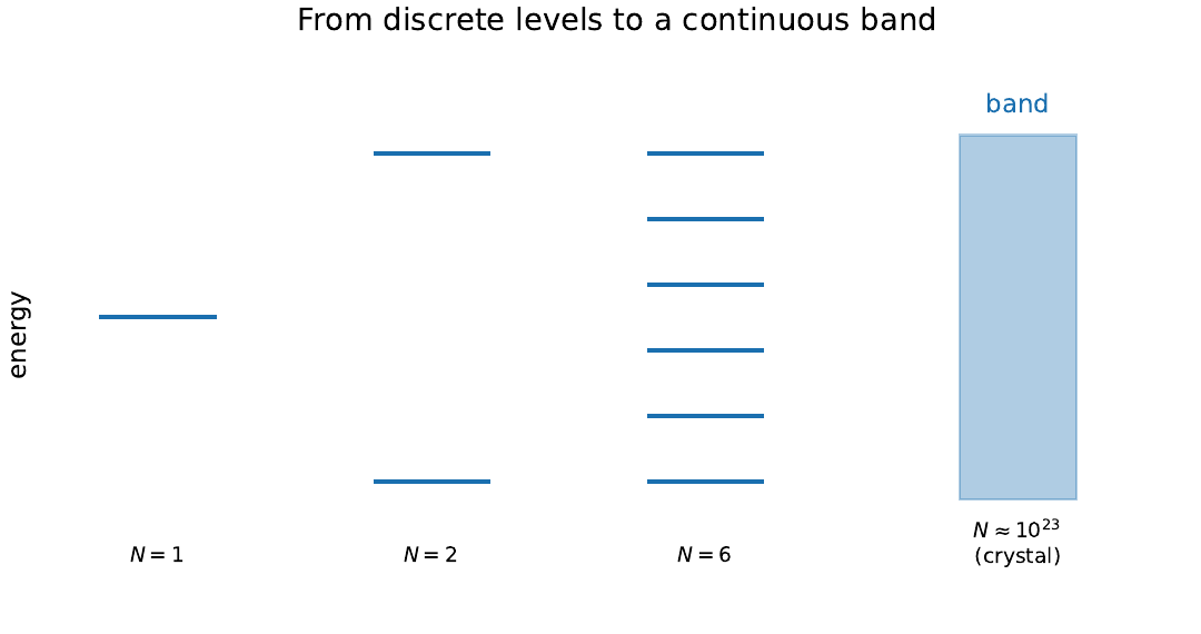
So the energy landscape of a solid looks like a layer cake: bands of allowed energies, separated by gaps of forbidden ones. Now pour in the electrons, from the bottom, two per seat, exactly as in the single atom. Where the filling stops is called the Fermi level. And here is the punchline of the whole story:
A completely full band carries no current.
Conducting means accelerating. An electron gains a tiny bit of energy from the applied voltage and moves to a slightly higher seat. In a full band there is no empty seat to move to, so every microscopic push is forbidden. The electrons are not stuck to their atoms; they are stuck in a fully booked theater. They can, in a quantum mechanical sense, move through the whole crystal, but for every electron drifting to the left there is a mirror partner drifting to the right, and the net current is exactly zero. A voltage cannot tip that balance, because tipping it would require moving someone to a free seat, and there is none.
Valence Band and Conduction Band
Two of these bands matter so much that they have names, and it is worth being precise about them.
The valence band is the highest band that is (essentially) fully occupied. Its name is no accident: it is formed from the outermost atomic orbitals, the valence orbitals, the same electrons that chemistry uses for bonding. These electrons are doing a job. In diamond, every valence electron is part of a carbon-carbon bond, and the valence band being full is just the band-picture way of saying “all bonds are saturated”. Full band, fully booked theater, no current.
The conduction band is the next band above it, and in an insulator or semiconductor it is (essentially) empty. An empty band carries no current either, for the trivial reason that there is nobody in it. But it is empty and has seats, and that combination is the key. Any electron that makes it up there has free seats in every direction and can be accelerated by even the smallest voltage. It behaves like the “free electron” from the school answer.
Between the two lies the band gap, and the entire electrical character of a material hangs on this one number:
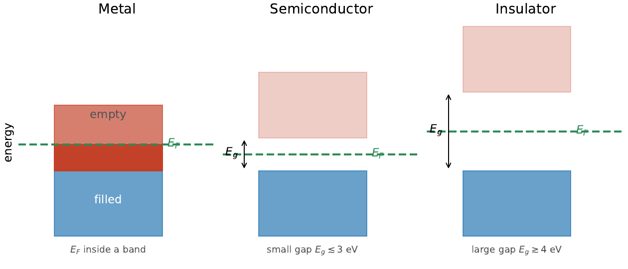
- In a metal like copper, the distinction collapses: the topmost occupied band is only half full, so valence band and conduction band are one and the same. Filled seats and empty seats touch at the Fermi level. There is no gap to cross, and the tiniest voltage moves electrons.
- In an insulator like diamond, the gap is huge, about 5.5 electron volts. Thermal jostling at room temperature hands out energy portions of about 0.025 electron volts, more than two hundred times too small. Practically no electron ever reaches the conduction band, and the material does not conduct.
- In a semiconductor like silicon, the gap is about 1.1 electron volts, small enough that at room temperature a rare thermal fluctuation occasionally lifts an electron across. That electron now conducts, and it leaves something behind: an empty seat in the otherwise full valence band, a hole. Neighboring valence electrons can now shuffle into that seat, the hole wanders, and it acts like a mobile positive charge. Conduction happens in both bands at once: electrons up top, holes below.
It is worth pausing on how lopsided this lottery is. Temperature does not gently warm up all electrons; it only rattles the ones sitting within about $k_B T \approx 0.025$ electron volts of the Fermi level. For an electron to cross a gap of 1.1 electron volts, dozens of these thermal portions have to pile up on one electron at the same moment, which is possible but rare, roughly a one-in-$10^{9}$ affair in silicon at room temperature. That is why the number of carriers in a semiconductor depends exponentially on the gap size and the temperature. Small changes have dramatic consequences: warm silicon up by a few tens of degrees and its conductivity multiplies, which is also why semiconductor circuits care so much about staying cool.
The carrier density can also be engineered instead of left to thermal luck: doping, the deliberate sprinkling-in of foreign atoms, plants extra electrons just below the conduction band or extra holes just above the valence band. Controlling the carrier density this way, region by region, is the entire trick that diodes, transistors, and every chip in your pocket are built on.
The Payoff: Calculating Copper
A story like this should be checkable. It is. The model gives a formula for conductivity, $\sigma = n e^2 \tau / m$: carrier density $n$, electron charge $e$ and mass $m$, and the average time $\tau$ between collisions with the vibrating crystal lattice. The formula tells a simple story: the voltage accelerates each carrier, a collision with a lattice vibration or a defect wipes out the gained speed after a time $\tau$ on average, and the resulting steady drift, multiplied by how many carriers there are, is the current. Between a metal and an insulator, $\tau$ and $m$ differ only by modest factors. What differs by more than twenty orders of magnitude is $n$, which is why the seating chart, and not some property of the individual electrons, decides everything.
For copper, the band picture makes a sharp prediction about $n$, and it is more interesting than it first sounds. A copper atom brings 29 electrons. The inner 18 sit in compact orbitals close to the nucleus; neighboring atoms are simply too far away for these orbitals to overlap, so their levels never broaden into bands worth the name, and their electrons stay home. The next ten fill the so-called d orbitals, which do overlap and do form bands, but those bands offer exactly ten seats per atom and copper delivers exactly ten electrons: completely full, and by now we know what a full band means. That leaves precisely one electron per atom, the outermost one, in a wide, half-full band. Twenty-eight spectators, one player. From copper’s density and molar mass, that yields $n \approx 8.5 \times 10^{28}$ conduction electrons per cubic meter. With the measured collision time $\tau \approx 2.5 \times 10^{-14}\,\mathrm{s}$:
\[\sigma = \frac{8.5\times10^{28} \times (1.60\times10^{-19})^2 \times 2.5\times10^{-14}}{9.11\times10^{-31}}\,\frac{\mathrm{S}}{\mathrm{m}} \approx 6\times10^{7}\,\frac{\mathrm{S}}{\mathrm{m}}.\]The measured value is $5.96\times10^{7}\,\mathrm{S/m}$. A staircase, a splitting rule, and a seating chart, and the number comes out right to within a few percent.
Going Deeper
Everything I hand-waved here, where the staircase comes from, why kinks cost energy, how the bands and the Fermi level are actually computed, is derived explicitly and with historical sources in the paper: From Atomic Orbitals to Energy Bands. The repository builds the PDF automatically, and all figures are generated from a single Python script. If this post made you curious, that is the next step of the staircase.
You can read the paper right here: