A Naive Comparator: Two NPNs, One PNP, and a SPICE Simulation to Prove It
Stephan BökelmannA while ago I posted a short video on Instagram in which I drew a naive analog-to-digital converter on paper and talked through it: a resistor ladder, a handful of comparators, one output line per comparator. Put a voltage on the input and the outputs go high from the bottom up, in proportion to that voltage. The result is a thermometer code, a flash ADC in its purest form, and it is the kind of circuit that makes the idea “analog in, digital out” click for people who have only ever seen it as a function call.
One of the questions that reached me afterwards was about the building block itself: what exactly does the comparator do, and why does it output either full supply or nothing? Fair question. In the video the comparator is a black box with two inputs and one output, and a black box is exactly what you should not accept when you want to understand a circuit.
I thought for a while about how to open that box. The honest textbook answer is “a comparator is an op-amp without feedback”, and I could have drawn an op-amp symbol and talked about open-loop gain. But that only moves the black box one level down: now the op-amp is the thing nobody understands. So I decided to go all the way and build the comparator from three discrete transistors, as a differential amplifier, and to simulate it, so that every claim in this article comes with a plot you can reproduce.
First, the transistors
A bipolar junction transistor (BJT) has three terminals: emitter, base and collector. For our purposes it is a current-controlled valve. A small current flowing into (or out of) the base lets a much larger current flow between collector and emitter. The ratio is the current gain, usually written as $\beta$ or $h_{FE}$, and it is somewhere between 100 and 300 for the small-signal parts used here:
\[I_C = \beta \, I_B\]You do not design around the exact value of $\beta$, because it varies wildly from part to part and with temperature, but you rely on it being large.
The second thing to know is that the base-emitter junction is a diode. It only conducts once the voltage across it reaches roughly 0.6 to 0.7 V, and above that the current rises exponentially with the voltage:
\[I_C = I_S \, e^{V_{BE}/V_T}, \qquad V_T = \frac{kT}{q} \approx 26\ \mathrm{mV}\]Every $V_T \ln 10 \approx 60$ mV more base-emitter voltage means ten times more collector current. That exponential is the whole reason a differential pair makes a good comparator, so keep it in mind.
NPN is the transistor you meet first. Its emitter points towards the negative rail (ground), its collector towards the positive rail. To turn it on, you pull the base about 0.65 V above the emitter. Current then flows from collector to emitter, conventional direction, into the collector and out of the emitter. In the schematic symbol the emitter arrow points outwards: “Not Pointing iN”.
PNP is the mirror image. Its emitter points towards the positive rail, its collector towards ground. To turn it on you pull the base about 0.65 V below the emitter. Current flows in at the emitter and out at the collector. The emitter arrow points inwards. If you hang a PNP’s emitter on the supply rail, it becomes a switch that connects its collector to the supply whenever something pulls its base down by a diode drop. That is exactly the job it has in this circuit: the NPN pair decides, the PNP delivers.
There is one more mode that matters here. If you drive a transistor’s base harder than needed to carry the collector current the external circuit allows, the collector-emitter voltage collapses to a few hundred millivolts and the transistor is saturated. A saturated transistor is a fine switch, but it is a slow one: the base region is flooded with charge that has to drain before the transistor turns off again. We will see the price of that in the last plot.
The repository
Everything for this article lives in
MaxClerkwell/naive-diff-amp-comperator
on GitHub. The circuit is described in Python with
SKiDL, which generates a KiCad
schematic and a KiCad netlist. Regular readers know that I consider this
the right way round: I made the case in
A Hill I Am Willing to Die On: HDL for PCB Netlists
that a schematic should be generated from a structured description, not
be the source of truth itself. I was also fairly harsh on SKiDL’s toolchain
in that article. For a circuit of this size it behaved, and the payoff is
exactly the one I argued for there: the same Python file produces the
netlist, the schematic and the SPICE deck, and the connectivity check at
the end proves that they agree. A small writer turns the SKiDL circuit and a
hand-written placement table into a .kicad_sch file, complete with the
Sim.* fields KiCad’s own simulator needs. Then a separate simulation
script takes that schematic, exports it to a SPICE netlist with
kicad-cli, and runs it through libngspice, the same library KiCad uses
internally. The whole run is two commands:
uv run komparator.py                          # SKiDL -> netlist + schematic, consistency check
uv run simulate.py komparator.kicad_sch       # schematic -> ngspice -> table + figures
The important property of this toolchain is that the schematic you look
at and the netlist that gets simulated cannot drift apart. The generator
re-exports the schematic with kicad-cli and compares its connectivity
against the SKiDL circuit; the run ends with
Schematic <-> SKiDL netlist: IDENTICAL. The simulation, in turn, reads
supply voltage, reference voltage and tail resistor straight from the
exported netlist. If you change a value in KiCad, that is the value that
gets simulated.
The schematic
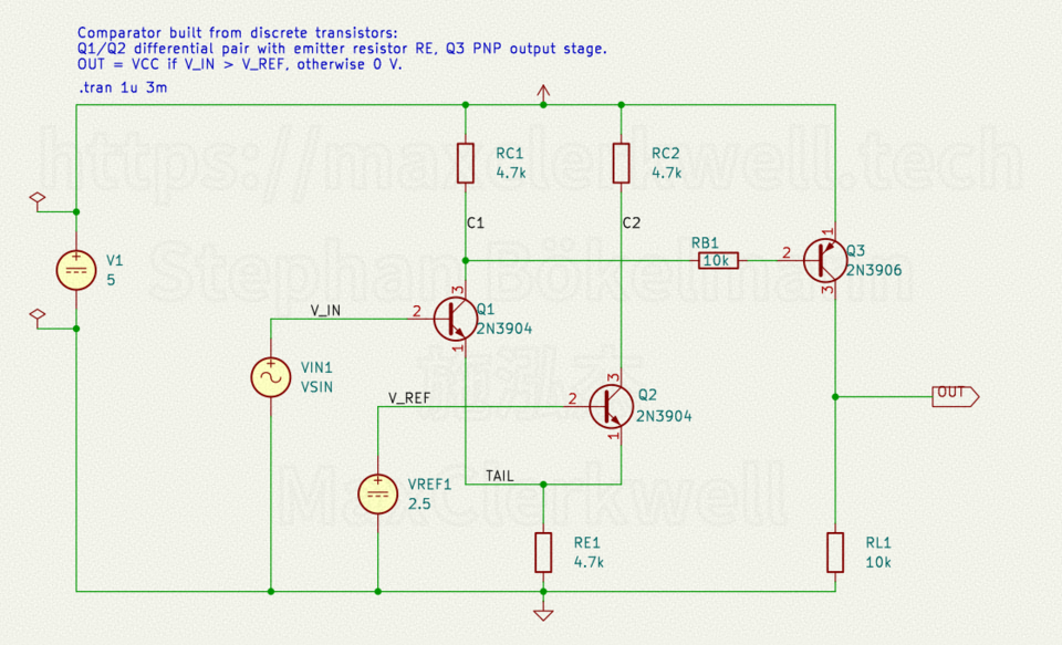
Reading it from left to right:
- V1 is the 5 V supply. VREF1 is the reference, 2.5 V, the voltage we compare against. VIN1 is the input; in the schematic it is a sine source so that the circuit can be simulated inside KiCad directly, the Python script overrides it per analysis.
- Q1 and Q2 are two 2N3904 NPN transistors. Their emitters are tied together at the node TAIL, which goes to ground through RE1 (4.7 kΩ). This is the differential pair. V_IN drives the base of Q1, V_REF the base of Q2.
- RC1 and RC2 (4.7 kΩ each) hang from VCC to the collectors, nodes C1 and C2. They turn the collector currents back into voltages.
- Q3 is a 2N3906 PNP. Its emitter sits on VCC, its base is driven from C1 through RB1 (10 kΩ), and its collector is the output node OUT, which RL1 (10 kΩ) pulls to ground.
Only C1 is used. C2 is there because the pair needs to be symmetric, and because watching C2 in the simulation makes the current steering visible.
How the differential pair compares
Start at the tail. Whatever happens at the inputs, the node TAIL sits one diode drop below the higher of the two base voltages, and RE1 turns that into a current. With $V_{REF} = 2.5$ V:
\[I_{tail} = \frac{V_{REF} - V_{BE}}{R_E} = \frac{2.5\ \mathrm{V} - 0.65\ \mathrm{V}}{4.7\ \mathrm{k\Omega}} \approx 0.4\ \mathrm{mA}\]That current has to come from somewhere, and the only places it can come from are the two collectors. The pair does not decide how much current flows; RE1 does that. The pair only decides how the current is split between Q1 and Q2.
The split is governed by the exponential we met above. Because both emitters are at the same potential, the ratio of the two collector currents depends only on the difference of the two base voltages:
\[\frac{I_{C1}}{I_{C2}} = \exp\!\left(\frac{V_{IN} - V_{REF}}{V_T}\right)\]Together with $I_{C1} + I_{C2} = I_{tail}$ this gives the familiar hyperbolic-tangent steering curve of the differential pair:
\[I_{C1} = \frac{I_{tail}}{2}\left(1 + \tanh\frac{V_{IN} - V_{REF}}{2 V_T}\right)\]At $V_{IN} = V_{REF}$ the current splits evenly, 0.2 mA each. Make $V_{IN}$ 60 mV higher and Q1 carries ten times as much as Q2; 120 mV higher and it is a hundred times. In practice the pair is fully steered to one side within about $\pm 4 V_T \approx \pm 100$ mV around the reference. Everything outside that narrow window is saturated in the logical sense: all of the tail current goes through one transistor, none through the other.
Now follow the current into the resistors. When Q1 carries all 0.4 mA, RC1 drops
\[\Delta V_{C1} = I_{tail} \, R_{C1} = 0.4\ \mathrm{mA} \times 4.7\ \mathrm{k\Omega} \approx 1.9\ \mathrm{V}\]so C1 sits at about 3.1 V. When Q1 is off, no current flows through RC1 and C1 sits at VCC. That is the signal that reaches the PNP: through RB1, Q3’s base is either at 5 V, the same as its emitter, and Q3 is off, or it is pulled about 1.9 V below the emitter, far more than the 0.65 V needed, and Q3 is hard on. In the first case RL1 pulls OUT to 0 V. In the second case Q3 connects OUT to VCC, less the small saturation voltage.
So the sign of $V_{IN} - V_{REF}$ determines which transistor gets the current, the collector resistor turns that into a swing of almost two volts, and the PNP turns that swing into a rail-to-rail output. Three stages, one comparison. The small-signal gain of the pair around the threshold is its transconductance times the collector resistor,
\[A_{pair} = g_m R_{C1} = \frac{I_{tail}}{2 V_T} R_{C1} \approx \frac{0.4\ \mathrm{mA}}{52\ \mathrm{mV}} \times 4.7\ \mathrm{k\Omega} \approx 36,\]and Q3 multiplies that by whatever its own stage adds. The total is high enough that the transition happens within a few millivolts, as the simulation will show.
Simulating it
The simulation script runs four analyses on the exported netlist:
- a DC sweep of V_IN from 0 to 5 V at V_REF = 2.5 V, the transfer characteristic,
- the same sweep for three different references, to see whether the threshold actually follows V_REF,
- a transient run with a 1 kHz sine of ±2 V around 2.5 V at the input,
- a transient run with a small pulse of only 200 mV overdrive, to measure propagation delay and edge times.
Each analysis is a couple of lines: load the netlist with the sources
replaced, run dc or tran, pull the node vectors out of ngspice and hand
them to Matplotlib. The transistor models are the usual Gummel-Poon
parameter sets for the 2N3904 and 2N3906 that circulate in every SPICE
library. The figures below are the ones the script writes to results/.
DC transfer characteristic
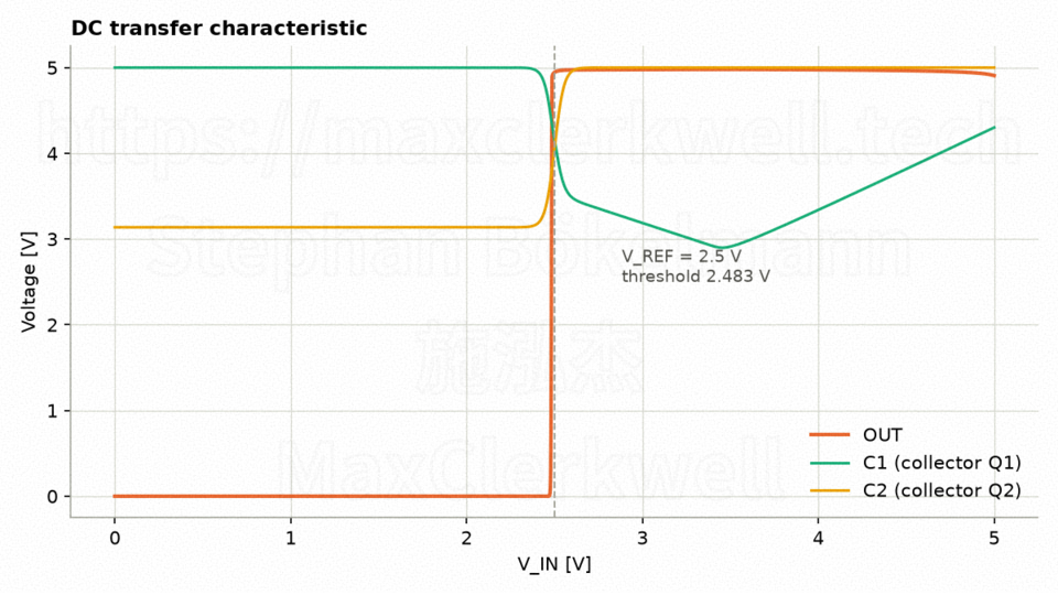
This is the plot that says “yes, it is a comparator”. The orange trace is OUT: zero for every input below the reference, 5 V for every input above it, and the transition is so steep that it looks like a vertical line. The script measures it: OUT crosses 2.5 V at an input of 2.483 V, and it takes 6.4 mV of input change to move the output from 10 % to 90 %. The maximum slope, the DC gain, is about 770 V/V.
The two collector traces are the part I find more instructive. At the left, C2 (yellow) sits at 3.1 V: Q2 carries the entire tail current and drops 1.9 V across RC2, while C1 (green) is at 5 V because Q1 is off. Around the threshold both traces swap places within a window of about 200 mV, exactly the ±100 mV steering range from the exponential. That is the current being handed from one transistor to the other.
Then C1 does something that a textbook differential pair does not: it keeps falling, reaches a minimum of 2.9 V at an input of about 3.4 V, and then climbs again, linearly, up to 4.3 V at 5 V input. The reason is that RE1 is a resistor, not a current source. As V_IN rises, TAIL follows it one diode drop below, and the tail current grows with it. More current, more drop across RC1, so C1 keeps sinking. But C1 cannot sink below the emitter forever: once C1 comes within a few hundred millivolts of TAIL, Q1 saturates, its base-collector junction starts to conduct, and from then on C1 simply rides along one saturation voltage above the emitter, which in turn rides along one diode drop below V_IN. That is the straight line on the right. It does not hurt the comparator, because Q3 is long since fully on, but it is the first hint that “naive” is the right word for the title.
The offset, 17 mV below the reference, comes from the fact that Q3 does not need C1 to drop all the way; a fraction of the swing is enough to turn it on, so OUT flips slightly before the pair is balanced.
The threshold follows V_REF
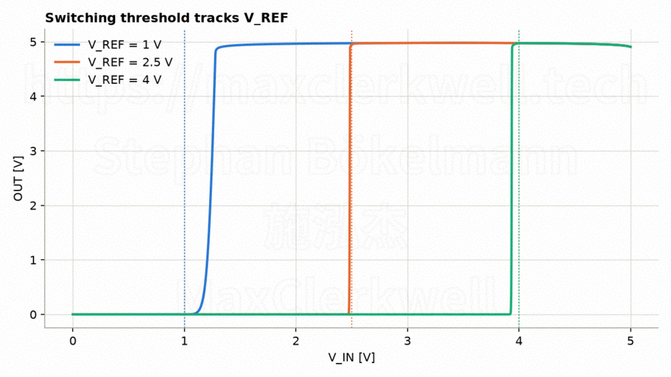
A comparator that only works at one reference is a Schmitt trigger with extra steps, so the second sweep moves V_REF around. At 2.5 V and 4 V the output is a clean step close to the reference: 2.483 V and 3.934 V, with transition widths of 6 mV and gains near 800 V/V. The offset at 4 V is larger, 66 mV, because the input pair is starting to run out of headroom: with the bases at 4 V and the emitters at 3.35 V, the collectors can only swing between 5 V and a bit above 3.35 V before Q1 saturates.
The 1 V curve is the interesting failure. The step is visibly softer, the threshold sits at 1.24 V, 240 mV above the reference, and the gain has collapsed to 70 V/V. Again the culprit is RE1. With V_REF = 1 V the tail node sits at only 0.35 V, so the tail current is 75 µA instead of 400 µA. That small current cannot pull C1 down far enough to turn Q3 on properly until $V_{IN}$ is well above $V_{REF}$, and the transconductance of the pair, $g_m = I_{tail} / 2V_T$, is five times lower, so the transition is five times wider. The fix is a standard one: replace RE1 with a current mirror or any other constant-current sink, and the tail current no longer depends on where the inputs happen to sit. I left it out on purpose. A resistor is what you would reach for on a breadboard, and this plot is exactly why real comparators do not.
A sine becomes a square wave
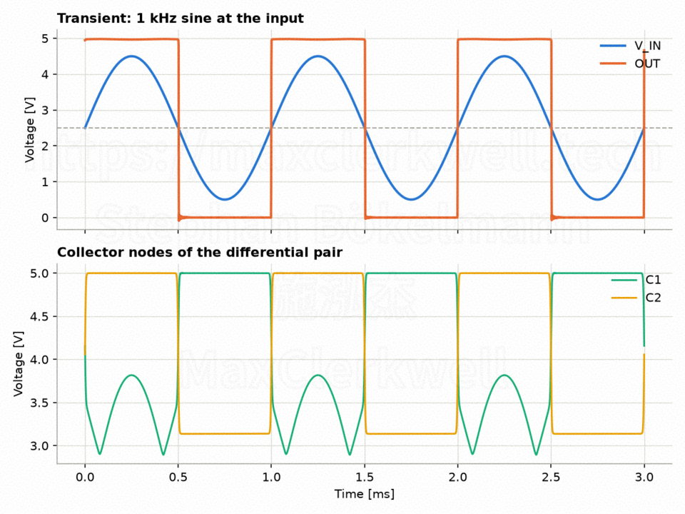
The transient run is the demonstration you would do on a bench: feed a sine in, watch a square wave come out. The top panel shows exactly that. OUT is high whenever V_IN is above the dashed 2.5 V line and low otherwise, and the script confirms that the duty cycle of the output is 50.4 %, which is the 17 mV offset expressed in time.
The bottom panel is the same time window seen from inside the circuit. C2 is the clean one: 5 V while Q2 is off, 3.1 V while Q2 carries the tail current, sharp transitions at each zero crossing. C1 is the mirror image, with the extra W shape during the high half-cycle. Read it together with the DC plot: as the sine rises through 2.5 V, C1 drops to about 3.4 V and keeps dropping to 2.9 V as the input climbs to 3.4 V. Beyond that, Q1 saturates and C1 tracks the input upwards, reaching 3.8 V at the sine peak of 4.5 V. On the way down it does the whole thing in reverse. None of that reaches the output, because Q3 is saturated the entire time, but it is a good reminder that the collector of a differential pair with a resistive tail is not a clean logic signal.
Pulse response: how fast is it?
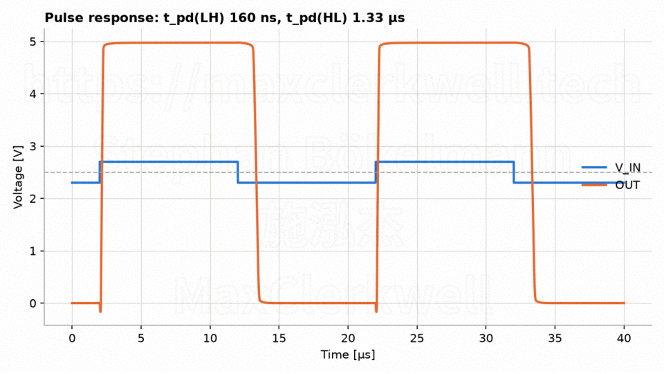
The last plot asks how quickly the comparator reacts when the input only just crosses the reference. The input is a pulse between 2.3 V and 2.7 V, so 200 mV of overdrive in each direction. The rising edge is fast: OUT crosses 2.5 V 160 ns after the input does, and it rises from 10 % to 90 % in 141 ns. The falling edge is a different story. It takes 1.33 µs, eight times longer, and it is visibly rounded.
That asymmetry is saturation, and it is the second time the word “naive” earns its place. When Q3 is on, its base is pulled 1.9 V below the emitter through a 10 kΩ resistor, which is far more base current than the load needs. Q3 is driven deep into saturation, and its base region fills with stored charge. When C1 rises again and the base drive disappears, that charge has to be removed before the collector current stops, and with only RB1 to drain it that takes about a microsecond. The same thing happens to Q1 whenever the input goes well above the reference, as the DC plot showed. A real comparator avoids this with a Baker clamp, a Schottky diode across base and collector, or by never letting the output transistor saturate in the first place, at the cost of not quite reaching the rail.
What “naive” buys you, and what it costs
Three transistors and five resistors, and the thing works: a switching threshold within 17 mV of the reference, a transition width of 6 mV, an output that goes from 0 V to 4.9 V. For the flash ADC in the video, where the references are a few hundred millivolts apart, that is more than enough. Put eight of these next to each other, feed the bases of the Q2s from a resistor ladder and the bases of the Q1s from the input, and you have the video’s circuit without a single integrated comparator.
The same simulation also shows, plot by plot, what a proper comparator does differently:
- A current source in the tail instead of RE1, so that the tail current and with it the gain and the offset do not depend on where the inputs sit. The 1 V curve in the second plot is the argument.
- No saturation in the output stage, so that turning off is as fast as turning on. The pulse response is the argument.
- A little hysteresis, some positive feedback from OUT back to the reference, so that a noisy input near the threshold produces one clean edge instead of a burst. That one you cannot see in these plots because the simulation has no noise, but anyone who has put a slow, noisy signal into a comparator without hysteresis has seen the output chatter.
Every one of those improvements is one more transistor or one more resistor, and every one of them is easier to appreciate once you have seen the version without it. If you want to try, the repository is the starting point: swap RE1 for a mirror, re-run the two commands, and watch the blue curve straighten up. Pull requests to naive-diff-amp-comperator are welcome, whether you add the current mirror, the Baker clamp or a better transistor model. And if you would rather argue about it than patch it, come find me on Discord.