open.cob.json: One File Between the Chip Designer and the PCB Designer
Stephan Bökelmann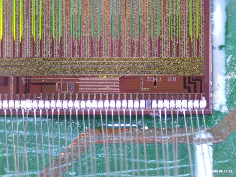
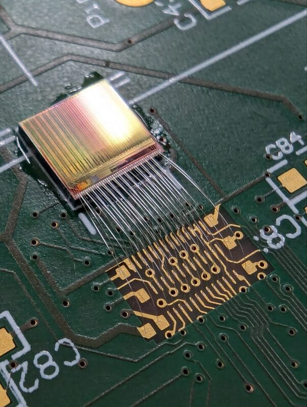
I have a folder that has been growing since my time at the Chair of Experimental Physics I in Bochum. It holds pad geometries that bonded well, force and time settings per wire and metal, a few SVGs of bonding plans, and the same three rules I have explained to every PCB designer I have worked with: no mask where the wire lands, no via under the die, keep the wire short and the angle sane. At some point I started writing this down as JSON, one file per chip, mostly so I would stop re-deriving it.
That folder was never in one place and never public. On 15 September I had a long call with Stuart Childs of wafer.space, whose customers are about to receive bare dies from a shared run and who will have to bond them. He asked, in effect, why the thing that ties the die to the board still lives in slides.
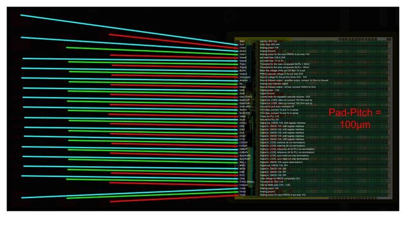
I did not have a good answer, so I spent the next two days turning the folder into a repository: open.cob.json. The README there says what it is and how to use it. This post is about the decisions that were hardest to make while writing it down.
A missing key is a lie
The first decision came from testing, not from design. If a file says nothing about the electrical specification of a wire, what does that mean? That the wire has none? That nobody wrote it down? A test system cannot tell, and it will either skip a measurement that should have happened or try to measure something that does not exist.
So the format forbids silence. A missing key is invalid. An empty object or
array is invalid. If something is absent, the file says "none", and that
is a design decision: no cutout, no paste on the fingers, no shear test. If
something is not known, the file says "unspecified", and that is a
documentation state: land patterns not yet designed, loop shape not yet
decided. A test system may not measure anything marked none, and must
flag anything marked unspecified as a missing spec. Electrical
specifications can never be none, because a wire always has electrical
properties. Either you give them or you admit you have not.
This sounds pedantic until you hand a file to someone else. A chip
designer can ship a file where the whole PCB side is "unspecified" and it
is valid. It is an honest description of what is known on the day the dies
leave the fab, and the PCB designer sees exactly where the work starts.
Geometry is not a property of a pad
My old JSON files described each PCB pad with a width, a length and a shape name. That broke the first time I needed a bond finger with a round probe area at the outer end, and it broke again when two projects wanted the same finger in different lengths.
The fix was to take geometry out of the pad entirely. A pad shape is now
its own file, <uuid>.shape.cob.json, and it contains nothing but
geometry: polygons per layer role, an origin the author picks, named
anchors such as the bond target, and a vertex tolerance. It is closer to
an SVG than to a footprint. The .cob.json file places a shape at a
position with a rotation and a scale factor, and the scale may differ in X
and Y. One finger shape serves every finger length. One paddle shape fits
every die.
I first put a catalog of “land patterns” between the shapes and the pads, each with process rules and a preference level. It lasted a day. It was a second place to say what a pad is, and every rule I wanted to hang on it belonged either to the pad instance or to the wire. The catalog is gone, the pad references the shape directly, and the rules sit where they apply.
Everything under the die is not one thing
The area under the die was another place where my old notes collapsed three different constraints into one. A cutout is a hole in the board. A via keepout is a prohibition. Required copper is an obligation. They are not variants of the same thing, and they are not properties of the die either. They are things on the PCB, on specific layers.
So the PCB block has a list of miscellaneous features, each with a kind, a shape, a position and the layers it applies to: mask opening, cutout, keepout with what it forbids, required copper with its net, fiducial. The die block only describes the die. This turned out to map cleanly onto KiCad: keepouts become rule areas, cutouts land on the edge cuts layer, and the rest are polygons on the layer they name.
Tolerances are the whole point of a validator
A die placed 50 µm off is normal. A bond target that was on copper in the nominal drawing may not be after that offset. My slides never said which tolerance applied to what, because slides do not have that column.
Every dimension in the format can be a plain number, a nominal with a symmetric tolerance, or a min-typ-max range. Die placement and PCB fabrication tolerances have their own block at the top of the file. The rule for a future validator is written down already: widen every bond target by the placement tolerance, shrink every copper polygon by the fabrication tolerance plus the shape’s vertex tolerance, and only then ask whether the wire lands.
What a real padframe taught the parser
The point of writing tools early was to find out where the format was wrong. The GDS importer found the first surprises.
I ran it on the
wafer.space gf180mcu example layouts.
The good news came first: 56 pad openings on the passivation layer, 52 of
them with a text label, and each label falls into exactly one opening. No
ambiguity at all. Then the two lessons. Searching for labels recursively
pulled in fourteen thousand internal pin labels from inside the I/O cells,
all on the same layer, so the pad names have to be taken from the top cell
only. And the naive way of finding which I/O cell a pad belongs to, by
asking which placed cell contains it, always answered “the metal fill
cell”, because fill covers the whole die. The right question is: which is
the smallest placed cell that contains this opening and itself contains a
pad opening. With that, the four unlabeled pads turned out to be the extra
dvdd and dvss pads, which the tool now marks as power pins with an
unspecified name.
The format was right about one thing here without my having planned it:
several pads may share a name, and a pad name may be "unspecified". A
padframe does that on its own.
The loop closes
The importer writes the die block. A small Tkinter editor loads that, shows the die, and lets me pick a shape and click pads onto the canvas. A generator turns the result into a KiCad 9 or 10 symbol and footprint, with the die on the silkscreen, custom copper pads with their mask polygons drawn exactly as specified, and the wires on a documentation layer. The same generator sits behind a button in the editor. I have opened the result in KiCad 10 and it looks like what I would have drawn by hand, in a few seconds instead of an afternoon.
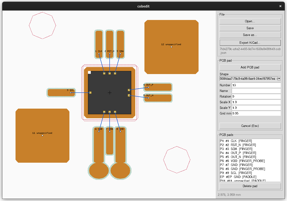

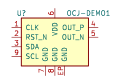
What the editor cannot do yet is add wires. What the repository cannot do yet is validate a file against a schema, or propose PCB pads from a die-only file using rules like the ones wafer.space publishes: no crossing wires, at most 45 degrees, one to three millimetres. Both are on the roadmap. Altium users will have to go through Altium’s KiCad importer, and I cannot verify that route myself.
Your chip, please
The best test for a format is a chip that is not mine. If you have a GDS or OASIS file of your own design, run it through the importer, open the result in the editor, place a few pads and export to KiCad. Then open an issue and tell me what broke or what the format could not express. The PDK name and a description of your padframe are enough; the layout does not need to leave your machine.
Everything is under CC BY 4.0. The folder is open now.